
The AND logic gate performs logical AND function. The output is HIGH (true) only when all the inputs are HIGH (true). Or in other words, if all inputs are non-zero, the output of this gate goes HIGH (non-zero). Or if any of the input is low the output remains low. There is a kit available on Amazon, that helps you to learn easily. Here is the logic gates learning kit. Don’t just read about the AND gate, test it yourself with the interactive AND gate simulator below.
Learning Objectives:
Introduction to AND logic, and digital building block
Introducing AND gate implementation using
AND Gate Simulator
Select a gate, toggle the inputs, and watch the truth table light up.
Truth Table
Working of AND gate:
In figure , the circuit symbol of 2 input AND gate, truth table and the waveforms or timing diagram of AND gate are also given. The output pulse rises from 0 to 1 when both inputs are high.

Case 1:
- Input A = 0
- Input B = 0
- Output = 0
Case 2:
- Input A = 0
- Input B = 1
- Output = 0
Case 3:
- Input A = 1
- Input B = 0
- Output = 0
Case 4:
- Input A = 1
- Input B = 1
- Output = 1
Now it is very easy to learn with the help of simulation software available. I always prefer to use multisim live it is quite easy and user friendly. Refer to figure 2, it shows AND gate simulation in multisim live. I have made a short video. Check it out.

Logical Expression of AND Logic Gate:
Y = A.B
Truth Table of AND Logic Gate:
The truth table of a 2-input AND gate shows all possible input combinations and their corresponding outputs:
| 2 Input AND Gate | ||
| Input A | Input B | Output |
| 0 | 0 | 0 |
| 1 | 0 | 0 |
| 0 | 1 | 0 |
| 1 | 1 | 1 |
How is an AND gate made?
Let’s delve deeper into constructing an AND gate using discrete components (switches, diodes and transistors). These methods, while less common in practical applications due to the availability of integrated circuits, is excellent for understanding the fundamental principles of how an AND gate works at a component level.
Logical AND Gate (Explain with the help of switches):

This is the switch model of AND logic. It is usually easy to understand the concept with the help of switches. In digital electronics diodes and transistors work as switches. So it is easy to grasp the concepts with the help of the switch model. Here you can see two switches connected in series. The input goes to the output only if both switches (switch A and switch B) are closed.
Implementation Using Diode Logic:
In modern electronics, it is ridiculous to implement this logic. But for beginners, it is necessary to understand the working of AND logic with the help of diodes.

Case 1:
It is seen in the schematic diagram, both inputs are tied to the ground. The positive side of the diode is connected to the positive side of the voltage supply. Both diodes are turned on and the current flows from the higher potential level to the lower potential level. The current will flow from the least resistive path. No current will flow from the LED and hence it remains off.
Case 2:
In this case diode, D2 is connected to the ground and D1 is connected to the 5V source. D2 is turned on. D1 is also tuned on. This is because the positive side of D1 is connected to the 7V source and the negative side is connected to the 5V source. Most of the current flow from D2 to ground and hence LED remains off.
Case 3:
The circuit working will be the same as in case 2.
Case 4:
In this case diode, D1 and D2 both are connected to a 5V source. Both the diodes are turned on. Only a little current flows from D1 and D2 because the potential difference is very low. The current flows from LED to ground. And hence LED turns on. The current and voltage values will be determined with the help of KVL.
Implementation AND Gate Circuit Using Transistor Logic:
In practical terms, BJTs are not suitable for switching. The specific circuit design can be more complex, the general idea is that transistors are used as switches to control the flow of current and achieve the AND logic function. Here we are interested to understand the logic or working of AND gate. It is easy to gain knowledge by practising different types of circuits on breadboards.

Case1:
Look at switches S1 and S2. Both are open. There is no voltage at the base. VBE = 0. The transistors are off. Output is low.
Case 2:
Look at switch S1, it is closed. Switch S2 is opened. Transistor Q2 is turned off. Now check the mode of each transistor. In digital switching devices BJT either works in saturation or cut off.
VBE > 0
The above condition is true. Transistor Q1 is ON Now check for the second condition.
VCE = VCE(sat) = 0.2V
VC is at a much higher potential than VE. So, Q1 is not in saturation.
Case 3:
It is the same as case 2.
Case 4:
Both switches are closed. Let’s look at Q2, base is at 5V, the emitter is grounded.
VBE > 0
Q1’s collector is connected to Q2’s emitter.
Q1’s Collector is connected to a 12 V source. Checking for the second condition,
VBC > 0
It is valid for both transistors.
Integrated Circuits (ICs):
In practice, AND gates are almost always implemented using integrated circuits (ICs). An AND gate IC contains multiple AND gates within a single package. Common examples include the 74LS08 (TTL logic) or the 4081 (CMOS logic) chips.
Frequently Asked Questions:
What is an AND gate?
The AND gate is a basic digital logic gate that outputs a high signal (1) only when all its inputs are high. It is particularly used in applications where conditions need to be met simultaneously.
How does an AND gate work?
An AND gate works by comparing two or more binary inputs. For example, if it has two inputs, it will output a 1 only if both inputs are 1. If either or both inputs are 0, the output will be 0.
What is an AND gate IC?
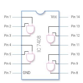
An AND gate IC (Integrated Circuit) is a small chip containing multiple AND gates. Common examples include the 7408 (a quad 2-input AND gate) in the 7400 series and 4081 in the CMOS series.
How many gates are there in an AND gate IC (7408 IC)?
The 7408 IC has four separate 2-input AND gates. Each gate can process a pair of inputs independently.
- 14-Pin Dual In-line Package (DIP)
- VCC (Pin 14) – Power Supply (+5V)
- GND (Pin 7) – Ground
- Remaining pins – Inputs and outputs for four AND gates
Are there alternatives to the 7408 AND gate IC?
Yes, there are several alternatives, such as the 4081 IC in the CMOS series, which performs similar functions but uses less power. Additionally, programmable logic devices (PLDs) can create customized AND gates as part of a larger programmable array
How is an AND gate implemented in CMOS technology?
In CMOS (Complementary Metal-Oxide-Semiconductor) technology, an AND gate is built using both NMOS and PMOS transistors. The PMOS transistors are in parallel, and the NMOS transistors are in series. This arrangement allows the gate to output a high signal only when both transistors are “on.”
What is the difference between an AND gate and an OR gate?
An AND gate outputs 1 only if all inputs are 1, whereas an OR gate outputs 1 if any input is 1. In short, the AND gate requires all conditions to be true, while the OR gate only needs one true condition to pass a high.
Can an AND gate have more than two inputs?
Yes, AND gates can have multiple inputs. While a standard IC like the 7408 provides 2-input gates, higher-input AND gates are possible and are often created by chaining multiple 2-input AND gates together.
Why are AND gates essential in digital circuits?
AND gates are fundamental for creating conditional logic, where multiple requirements must be met before activating a specific action. They’re essential in circuits that perform tasks such as data comparison, signal control, and basic arithmetic operations.
Recommended Books
Digital Design: With an Introduction to the Verilog HDL
Digital Fundamentals 11th ed. Edition
Digital Design and Computer Architecture, RISC-V Edition: RISC-V Edition 1st Edition
zafarimamalvi@hotmail.com