
An adder is the fundamental building block of many digital systems. An adder is a digital circuit that performs the addition of two numbers. It is easy to design and made up of simple logic gates. A binary adder is a circuit that performs addition on binary numbers only. A parallel binary adder circuit means all the inputs are available simultaneously, and processing each bit position is in parallel. This is in contrast to a serial adder, which adds binary numbers one bit at a time, processing each bit sequentially.
Topics:
Design a half adder circuit using
XOR gate
Basic logic gates
NAND gates
NOR gates
Design a one bit full adder
Input and output
Block diagram
Truth Table
Karnaugh Map to get simplified SOP expression for full adder logic
Circuit diagram from the simplified logic expression
FAQs
Delay associated with ripple carry adder
Design a half-adder circuit:
A half adder is a circuit that accepts two binary inputs (let’s suppose A and B) of one bit. It produces two outputs (sum and carry) of one bit. For two inputs there are 22 possible input combinations.
Here,
The input variables are designated as augend (A) and addend (B) bits. The output variables are sum (S) and output carry (CO).
The following truth table and illustration depict the same.

| A | B | Sum = S | Carry = C |
| 0 | 0 | 0 | 0 |
| 0 | 1 | 1 | 0 |
| 1 | 0 | 1 | 0 |
| 1 | 1 | 0 | 1 |
From the truth table, there are many possible ways to implement a half-adder. In this tutorial, the half-adder circuit is implemented in many different ways and drives their expressions as well.
- Half adder circuit using XOR gate
- Half adder circuit using NAND gates
- Half adder circuit using NOR gates only
- Half-adder circuit using basic logic gates
Half adder circuit using XOR gate:
This is the simplest possible implementation of a half-adder circuit. It employs only two logic gates. A and B are the two inputs. Sum and Carry are the two outputs.


Half adder circuit using basic logic gates:
The half-adder circuit can be implemented using basic logic gates. It requires 3 AND gates, an OR gate and two inverters.

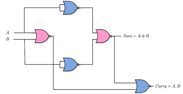
Design a half-adder circuit using NAND gates only and drive its expression:
Five NAND gates are required to implement a half-adder circuit.


Half adder circuit using NOR gate and drive its expression:
Five NOR gates are required to implement a half-adder circuit.

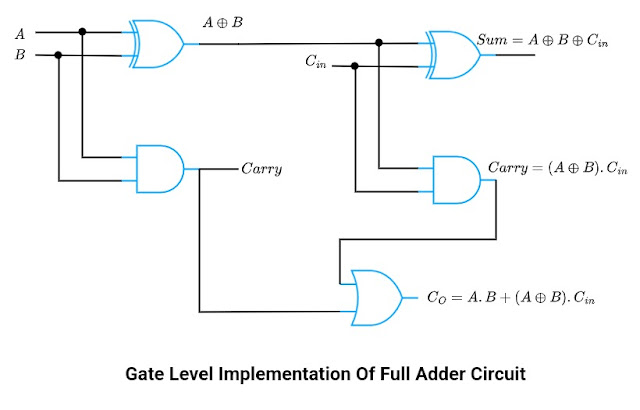
Design a one-bit full adder with two half adders and an OR gate:
There are many techniques to implement full adders. But it is an introductory article on binary adders. It is better to start with the simple adder circuit. This full adder circuit consists of two half adders and an OR gate. It is capable of adding three 1-bit binary numbers. Two of them are inputs (A and B). The third binary number is a carry-in.
There are various steps involved in designing a full adder.
- Input and output
- Block diagram
- Truth Table
- Karnaugh Map to get simplified SOP expression for full adder logic
- Circuit diagram from the simplified logic expression
Input And Output:
It is an adder circuit. It will accept two inputs A and B. It performs the addition of A and B. Then it will produce two outputs sum (S) and carry (COUT). It will also accept carry from the previous stage. Have a look at the addition of two numbers.
Block Diagram:
The block diagram is given below. The block diagram given below shows the full adder takes two binary numbers (A and B) as input. Both inputs are 1-bit numbers. There is a carry input as well. It is also 1-bit long. So, there are a total of three inputs, each input is only 1-bit long. There are two outputs S and COUT (sum and carry respectively). Both outputs are 1-bit long. There is an “add” circuit that performs addition on two binary numbers. The block diagram helps to visualize the internal workings of the full adder and its relationship to the inputs and outputs.
This adder is a building block of higher-bit adders. This is known as a one-bit full adder.

Truth Table:
Below is the truth table and an illustration. It shows how the addition of three binary numbers is carried out. The output represents the sum of three binary numbers.

| A | B | C | S=A⊕B⊕Cin | CO =A.B+(A⊕B)Cin |
| 0 | 0 | 0 | 0 | 0 |
| 0 | 0 | 1 | 1 | 0 |
| 0 | 1 | 0 | 1 | 0 |
| 0 | 1 | 1 | 0 | 1 |
| 1 | 0 | 0 | 1 | 0 |
| 1 | 0 | 1 | 0 | 1 |
| 1 | 1 | 0 | 0 | 1 |
| 1 | 1 | 1 | 1 | 1 |
From the truth table, we can conclude that a single full adder consists of three inputs. Two inputs are the two binary numbers A and B (one bit) and the third input is the carry from the previous half-adder.
Karnaugh Map For Full Adder Circuit:


The implementation of a one-bit full adder circuit is given below:

Some Frequently Asked Questions:
What are 1-bit full adders? How many full adder blocks are required?
It is an adder that can add two 1-bit numbers. There is an additional input, that is carry input. This is the carry generated from the previous adder. There are two outputs, sum and carry. It comprises two half-adders. And an OR gate. To add two 1-bit binary numbers there is only one full adder required. Keep in mind that the bit width of each input is 1 bit. The figure is given below.

What are 2-bit full adders?
The block diagram is given below. From the block diagram given below, the 2-bit full adder takes two binary numbers (A and B) as input. Both inputs are 2-bit numbers. Two 1-bit full adders are required. Each full adder is capable of adding three 1-bit numbers.
There is a carry input as well. It is 1 bit long. So, there are a total of three inputs, input A and B are 2-bit long. There are two outputs S and CO (sum and carry). The sum (S) is 2-bit long and COUT is 1-bit long. The truth table for a 2-bit full adder would have 32 entries, one for each possible combination of inputs.


What are 3-bit adders?
The block diagram is given below. From the block diagram given below, the 3-bit full adder takes two binary numbers (A and B) as input. Both inputs are 3-bit numbers. Three 1-bit full adders are required. Each full adder is capable of adding three 1-bit numbers.
There is a carry input as well. It is 1 bit long. So, there are a total of three inputs, input A and B are 3-bit long. There are two outputs S and CO (sum and carry). The sum (S) is 3-bit long and COUT is 1-bit long. The truth table for a 3-bit full adder would have 128 entries, one for each possible combination of inputs.

What are 4-bit adders?
The block diagram is given below. From the block diagram given below, the 2-bit full adder takes two binary numbers (A and B) as input. Both inputs are 4-bit numbers. Two 1-bit full adders are required. Each full adder is capable of adding three 1-bit numbers.
There is a carry input as well. It is 1 bit long. So, there are a total of three inputs, input A and B are 2-bit long. There are two outputs S and CO (sum and carry). The sum is 4-bit long and COUT is 1-bit long. The truth table for a 2-bit full adder would have 256 (2n, where n = number of input bits) entries, one for each possible combination of inputs. Here are 9 inputs applied to four full adders.


What are n-bits adders?
In the same way, the n-bits full adders comprise of n-full adders. Both inputs A and B are n-bits long. The sum is also n-bits long. The carry output is 1 bit long.
What are parallel binary adders?
All the above-mentioned adders are parallel binary adders. The parallel binary adders are built from full adders linked together in a cascade, with each adder’s output carry wired to the input carry of the one that comes after it. For a four-bit number, there are four full adders required. For an n-bit number, there are n full adders required.
Delay Associated With Ripple Carry Adder:
In this section, I will discuss the propagation delay associated with ripple carry adder. After understanding this part you will be able to calculate propagation delay.
Let’s suppose there are two binary numbers.
A is the augend, bit width: 4
B is the augend, bit width: 4
Ci is an input carry
COUT = output carry are the output
C1, C2, and C3 are the intermediate carry signals generated from the intermediate stages.
Looking at the dock diagram, at the initial State, this circuit has 9 inputs

There are 2 inputs for each full adder. There are 4 adders, and each full adder has three inputs. The first full adder is provided with an input carry. The rest of the full adders have to wait for carry generation.
The second full adder will generate the correct output when there is a carry generated by the first full adder.
The same is true for other full adders as well. Each full adder accepts the carry from the previous stage.
Each full adder has to wait for the carry signal.
There must be some delay associated with the circuit. The total propagation time is equal to the propagation delay of a gate times the number of gate levels in the circuit.The maximum propagation delay time in an adder circuit is defined as
“The time it takes the carry to propagate through the full adder.”
It is quite obvious that the signal has to travel through several gates. The signal from input carry Cin has to travel through an AND gate and an OR gate. Check out the path of Cin.

Gate Levels
There are two gate levels for a one-bit full adder.
For a two-bit adder, there are 2×2 gate levels for the carry to propagate from input to output.
For an ‘n’ bit full adder, there are 2n gate levels for the carry to propagate from input to output.
The propagation time of the carry signal from input to output increases with an increase in the number of input bits. Or in other words, as the number of bits increases, the number of parallel connected full adders increases. And hence propagation time of the carry signal from input to output also increases. This is the limiting factor on the speed with which two numbers are added.
Conclusion:
Parallel binary adders are essential components of digital systems, performing binary addition operations on multiple pairs of binary numbers simultaneously. The ripple carry adder is simple to implement, but it suffers from a carry propagation delay that limits its performance.
Attempt quiz on Parallel Binary Adders.
Richmond consulting firms
Fiza Rehman