
The first simplest and most fundamental logic circuits used in digital electronics is a buffer. A buffer is a single-input, single-output logic gate. The output is exactly same as the input. In essence, a buffer is a device that amplifies or strengthens the signal it receives. While it does not change the logic state of the input (it passes a “1” or “0”). In other words, it does not invert or alter the logic state. If the input is logic “1”, the output will also be logic “1”, and if the input is logic “0”, the output will be logic “0”. Essentially, it passes the signal through unchanged. It ensures the output is strong enough to drive other circuits. Buffers are used when signal integrity is critical. For example, it is essential in cases where the output needs to travel over long distances or drive multiple devices.
Learning Objectives:
- How Does a Buffer Work?
- Circuit Symbol
- Logical expression
- Introducing buffer implementation using
- Switches
- Three different ways to implement the buffer logic
- CMOS
- FAQs
Circuit Symbol:

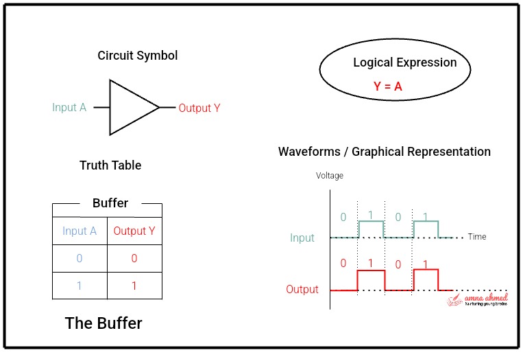
The logic symbol is represented by a triangle pointing to the right. The input is A, which is shown on the left side, whereas output is on the right side. This symbol is similar to the symbol for an amplifier. As compared to the NOT gate, there’s no negation symbol (the small circle at the output side) because it doesn’t invert the signal.
Logical expression and truth table:
The logical expression of a buffer is straightforward because the output is always the same as the input. A buffer does not modify or invert the input signal but simply passes it through to the output.If we denote the input of the buffer as A and the output as Y, the logical expression is:
Y = A
| Input A | Output Y |
| 0 | 0 |
| 1 | 1 |
This means that whatever value the input A holds (either 0 or 1), the output Y will hold the same value. There is no complex logic involved in a buffer. But still it is considered as the logic gates in digital electronics.
Types of Buffers
There are a few types of buffers, each with a slightly different application:
- Non-Inverting Buffer: This is the basic type of buffer, where the output is the same as the input.
- Tri-state Buffer: This buffer has an additional control input. A tri-state buffer has three output states: high, low, and high-impedance (Z). Or the outpu states are represented by: 0, 1, or high impedance (disconnected state). The high impedance state is useful in bus systems, where multiple devices share the same connection.

The Switch Model of a Buffer:
In practical life, we never use a switch as a buffer. The purpose of a switch model is to explain easily. Just like a switch, its purpose is to transfer the input to the output. Imagine the buffer as a single-pole single-throw (SPST) switch that connects the input directly to the output. This switch is “closed” when the input is present (logic 1), allowing the signal to pass through, and “open” when there’s no signal (logic 0).
How it works in steps:
ON State: When the input is high (logic 1), the switch closes, allowing the signal to pass directly to the output. So, the output becomes high (logic 1), mirroring the input
OFF State: When the input is low (logic 0), the switch opens, resulting in a low output (logic 0). This way, the output matches the input .

Three different ways to implement buffer logic:
There are so many different ways to implement the buffer logic. We will limit our study to a very basic buffer circuit. In digital circuit design, there are various ways to implement the buffer.
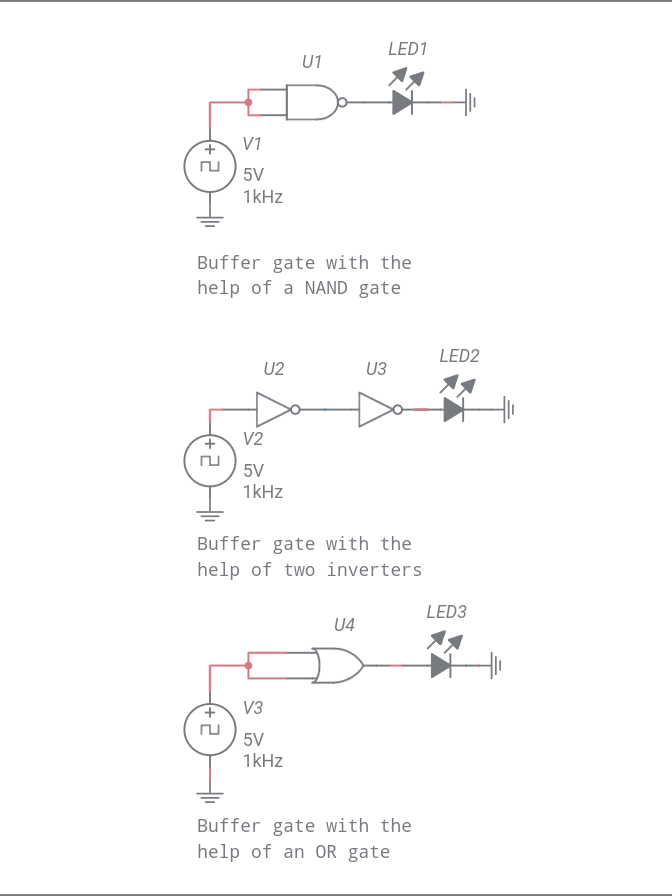
Two inverters in series can act as a buffer:
Simple and easy task. Two inverters in series will produce the same logic as that of input. In this way the input inverses two times and the output is the same as that of the input.
Buffer with the help of an AND gate:
Consider a two-input AND gate. Connect both of its input terminals. It works as a buffer. Have a look at the schematic diagram.
Buffer with the help of an OR gate:
Consider a two-input OR gate. Connect both of its terminals. It will act as a buffer.
Note: there is a difference between input wave and output wave amplitude. This is because every practical circuit experiences a voltage drop. The drop is due to the internal circuitry of the logic gates.
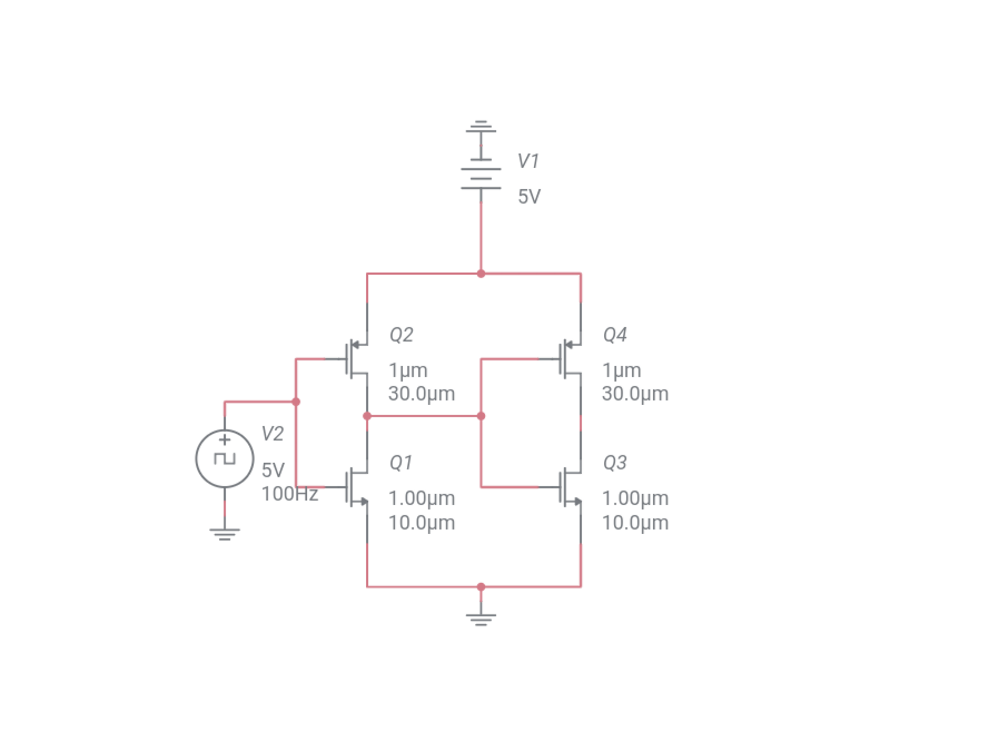
Implementation Using CMOS Logic
Two back to back inverters work as a buffer.
Frequently Asked Questions :
1. What is a buffer in digital electronics?
A buffer is a basic logic gate that transmits the input signal to the output without changing its value or logic state. It strengthens or isolates the signal while maintaining its logic state.
2. What is the main function of a buffer?
The primary function of a buffer is to pass the input signal to the output unchanged. It is used to boost the signal strength or provide electrical isolation between circuit stages.
3. How does a buffer differ from an inverter?
A buffer transmits the input directly to the output without changing its state. On the other hand, an inverter (NOT gate) flips the input signal, outputting the opposite logic state (0 becomes 1, and 1 becomes 0).
4. Why is a buffer used in circuits?
Buffers are used for several reasons, including:
- It strengthens weak signals
- It provides isolation between different parts of a circuit
- It is used to introduce slight delays for timing purposes.
5. What is the symbol of a buffer?
The symbol of a buffer is a triangle pointing to the right, resembling the symbol for an amplifier. It doesn’t have a negation.
6. What is the number of buffer logic gate IC?
The name of the IC commonly used as a buffer logic gate is Hex Buffer/Driver IC. A widely used example is the 7407 IC, which belongs to the 7400 series of TTL logic gates.
- IC Name: Hex Buffer/Driver
- IC Number: 7407
- Features:
- Contains six independent buffers.
- Provides high current output.
- Useful in interfacing digital circuits to higher current loads.
This IC is commonly used for signal amplification and driving larger loads in digital circuits.
What is the difference between normal buffer and tri state buffer?
The primary difference between a normal buffer and a tri-state buffer lies in the number of possible output states and how they interact with a shared communication bus.
| Feature | Normal Buffer | Tri-State Buffer |
| Output States | 2 States: High (1) Low (0) | 3 States: High (1) Low (0), High-Impedance (Hi-Z). |
| Control Pin | None | Enable (EN) |
| Bus Usage | Cannot share a bus | Ideal for shared buses |
| Analogy | A light switch that is always either On or Off. | A light switch that can be On, Off, or completely unplugged. |
Why do we need a tri state buffer?
In digital electronics (like VLSI design), multiple devices often need to send data over a single wire or we can called it as a bus.
- Normal Buffers are always on. If two normal buffers try to send different signals (one High, one Low) to the same wire, they will fight each other, causing a short circuit and high heat.
- Tri-State Buffers solve this with the High-Impedance (Hi-Z) state. When the “Enable” pin is inactive, the buffer effectively disconnects from the circuit. This allows one device to talk while others “stay off,” ensuring smooth data flow without interference.
Recommended Books:
Digital Design: With an Introduction to the Verilog HDL
Digital Fundamentals 11th ed. Edition
Digital Design and Computer Architecture, RISC-V Edition: RISC-V Edition 1st Edition